
Designing your own circuit boards might seem like a daunting task, especially for those without a formal background in electronics. However, software like PCB Artist aims to simplify this complex process, making it accessible even to beginners. This user-friendly program offers a fully integrated solution for schematic capture and PCB layout, guiding you through each step with intuitive wizards and helpful tools. This article explores the features and functionalities of PCB Artist, detailing its strengths and limitations, and providing insight into its potential as a valuable tool for both hobbyists and students.
Navigating the Design Process: A Step-by-Step Guide
PCB Artist streamlines the circuit board design process into five manageable steps, each supported by helpful wizards that guide users through the necessary parameters and settings. This approach significantly reduces the learning curve associated with professional PCB design software. Let’s examine each step in detail:
1. Circuit Design: Utilizing the Integrated Schematics Capture Tool: The initial phase involves designing the circuit itself. PCB Artist provides an integrated schematics capture tool that simplifies the process of creating a visual representation of your circuit’s components and their interconnections. This tool utilizes a drag-and-drop interface, allowing users to easily place components on the workspace and connect them using virtual wires. The software’s library contains a range of common electronic components, making it easy to find the parts you need. A comprehensive tutorial is included to assist users unfamiliar with schematic capture, ensuring a smooth onboarding experience. This tutorial walks users through the basics, from component placement and wiring to the proper use of symbols and annotations, making even the initial stages of design accessible. The intuitive nature of the interface minimizes the need for prior experience with similar software.
2. Defining the PCB Parameters: A Wizard-Driven Approach: Once the schematic is complete, the next step involves defining the physical parameters of the PCB itself. This critical stage sets the stage for the subsequent layout process. PCB Artist utilizes a wizard to guide users through the process of defining key parameters such as:
-
Number of Layers: This dictates the complexity of the PCB and the number of copper layers available for routing traces. Beginners typically start with a simpler double-sided board, while more advanced designs might require multiple layers for increased complexity and density. The wizard provides clear explanations of the implications of each choice, allowing users to make informed decisions based on their design requirements.
-
Track Sizes: This refers to the width of the copper traces that connect the components. Choosing the appropriate track size is critical for ensuring signal integrity and managing current flow. The wizard offers guidance on selecting suitable track sizes based on the type of signal and current requirements of each component. This ensures the final design meets performance expectations.
-
Board Dimensions: Users must define the overall dimensions of the PCB to accommodate all components and traces. This step is crucial for proper fabrication and ensures the final product meets physical constraints. The wizard helps users estimate the required board size based on the placement of components in the schematic. Users can then manually adjust the dimensions as needed.
The wizard’s structured approach ensures that users consider all essential parameters before proceeding to the layout phase, minimizing errors and improving design efficiency.
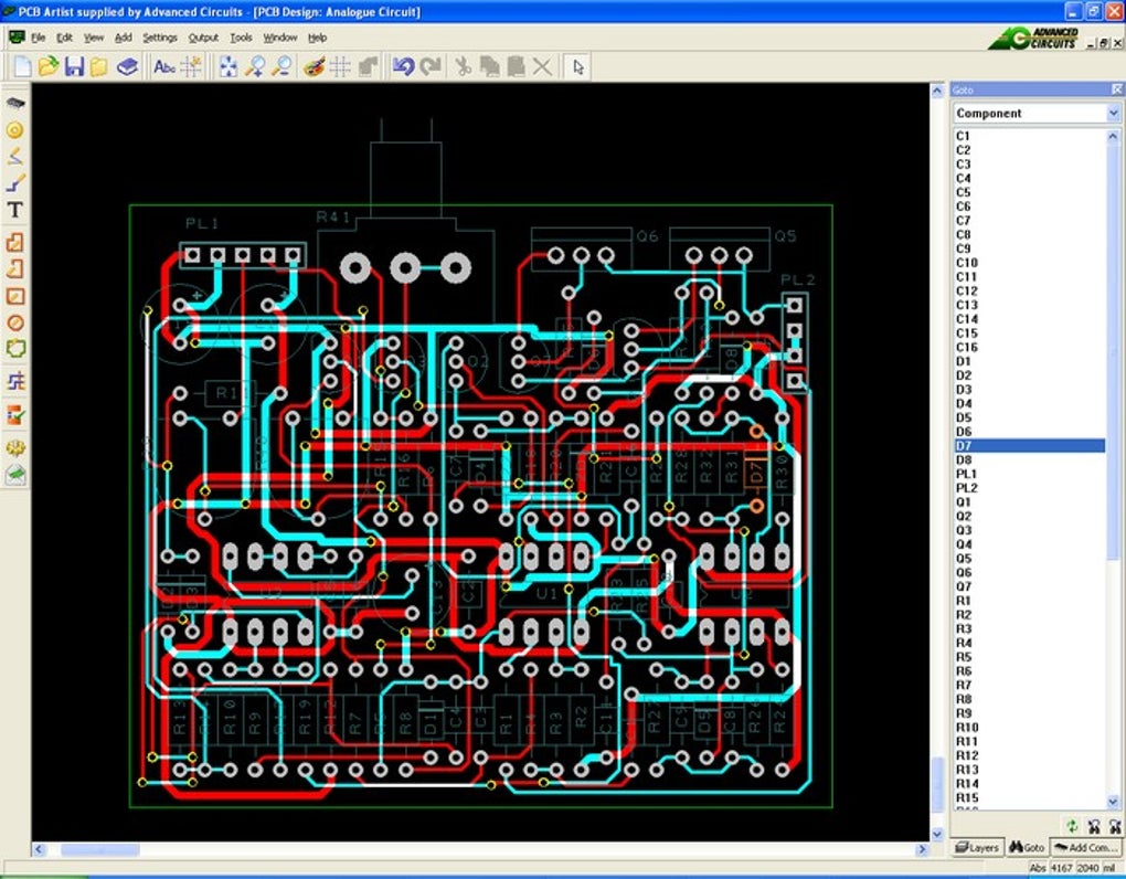
3. PCB Layout: Leveraging Autoplacement and Autorouting: The core of the PCB design process is the layout phase, where components are physically placed on the board, and connections are routed using copper traces. PCB Artist simplifies this challenging task through the integration of autoplacement and autorouting features.
-
Autoplacement: This automated feature intelligently arranges components on the board, striving for an optimal placement that minimizes trace lengths and improves overall design efficiency. While not always perfect, autoplacement provides a solid starting point that can then be manually refined to meet specific design requirements. Users can manually adjust component positions, fine-tuning the layout for better aesthetics or to address specific routing challenges.
-
Autorouting: This automated routing feature connects the components based on the schematic, automatically generating the necessary copper traces. The algorithm aims to create a clean and efficient routing scheme while adhering to the design rules defined in the previous step. Similar to autoplacement, autorouting serves as an excellent starting point that can be further optimized by the user. Manual intervention may be needed to refine certain connections or to manage trace congestion in complex designs.
4. Generating a Bill of Materials (BOM): Streamlining Procurement: Once the layout is complete, PCB Artist automatically generates a BOM that lists all the components used in the design, along with their relevant specifications. This crucial document simplifies the procurement process, allowing designers to easily order all the necessary parts from suppliers. The BOM typically includes information such as part numbers, quantities, and manufacturers, ensuring a streamlined process.
5. Design Verification and Manufacturing: Before submitting the design for manufacturing, PCB Artist performs automated design rule checks (DRC). This process automatically verifies that the design meets the specified design rules, identifying any potential issues such as shorts, opens, or clearance violations. Identifying these potential problems early in the design process avoids costly manufacturing delays. The software flags potential problems, allowing the designer to make necessary corrections before proceeding. The program then encourages the user to submit their finalized design for manufacturing. Although this is optional, it provides a convenient path for those wanting to bring their designs to life.
Strengths and Limitations of PCB Artist
PCB Artist excels as a beginner-friendly tool due to its intuitive interface, comprehensive wizards, and integrated design verification features. Its streamlined workflow and ease of use make it an ideal choice for hobbyists, students, and anyone seeking an accessible entry point into PCB design. The software’s automated features, such as autoplacement and autorouting, significantly reduce the time and effort required to create functional designs.
However, the software’s simplicity also presents certain limitations. Its capabilities may prove insufficient for designing highly complex circuit boards with numerous components, advanced routing requirements, or intricate high-speed signal pathways. Advanced users might find the limited customization options restrictive, and the automated features, while convenient, might not always produce optimal results for all designs. In such scenarios, professional-grade PCB design software offering greater control and customization might be necessary.
Therefore, PCB Artist is best suited for projects of moderate complexity. It serves as an excellent learning tool and allows for the creation of many practical circuit boards. However, users undertaking highly complex projects may need to explore more advanced software options.
Comparison with Other PCB Design Software
Several other PCB design software options are available, each with its strengths and weaknesses. Comparing PCB Artist with other choices highlights its unique position in the market:
-
KiCad: This open-source software offers a comprehensive set of features and is suitable for complex designs. However, its interface is more challenging to master, requiring a steeper learning curve than PCB Artist.
-
EasyEDA: This cloud-based software offers a similar level of ease of use to PCB Artist, but with advanced features for more complex projects. It also allows for collaborative design.
-
DipTrace: This commercial software boasts a powerful feature set and user-friendly interface, but comes at a cost. This is a more substantial investment compared to the free PCB Artist.
-
Altium Designer: This professional-grade software is used for highly complex designs, requiring significant expertise and incurring considerable licensing fees.
The choice of software depends on the project’s complexity, the user’s experience level, and budget constraints. PCB Artist shines in its simplicity and accessibility, providing an excellent entry point into PCB design for beginners, while more complex projects may necessitate using more advanced, albeit steeper learning curve software packages.
Conclusion: An Accessible Gateway to Circuit Board Design
PCB Artist provides a valuable and accessible gateway to the world of PCB design. Its intuitive interface and guided workflow significantly reduce the complexity of this challenging task, making it suitable for a wide range of users, from hobbyists to students. While it has limitations in terms of handling highly complex projects, its strengths lie in its ease of use, comprehensive tutorials, and automated features. For those new to PCB design or seeking a simple yet effective tool for moderately complex projects, PCB Artist presents a compelling and user-friendly option. Its free availability makes it an ideal platform to experiment with circuit board design and learn the fundamental concepts before potentially moving on to more advanced software if required.
File Information
- License: “Free”
- Version: “1.0.16”
- Latest update: “July 12, 2019”
- Platform: “Windows”
- OS: “Windows NT”
- Language: “English”
- Downloads: “63.8K”
- Size: “24.22 MB”


